High-efficiency silicon solar cells continue to push performance boundaries, with interdigitated back-contact (IBC) architectures standing out for their ability to eliminate front-side shading and maximize light absorption. However, translating these designs into scalable manufacturing remains challenging, particularly when it comes to forming precisely controlled n⁺ and p⁺ poly-Si passivating contacts on the rear side.
Inkjet printing has emerged as a promising, lithography-free alternative that could simplify fabrication and reduce costs. Yet, its adoption has been hindered by two critical issues: unintended doping in nominally intrinsic regions, and cross-doping between adjacent structures during thermal processing.
A recent study by Jiali Wang and collaborators, conducted in partnership with CAMECA, demonstrates how a spin-on SiOₓ capping layer can effectively mitigate these challenges. Just as importantly, it showcases the key role of dynamic secondary ion mass spectrometry (SIMS), in providing the insight needed to understand and optimize this process.
Why Dynamic SIMS is Essential
Accurate control of dopant distributions in advanced devices demands both ultra-high sensitivity and fine spatial resolution, a combination uniquely delivered by dynamic SIMS.
Using the
CAMECA IMS 7f-Auto platform, researchers performed high-resolution dopant mapping and depth profiling, capturing complete 2D + depth distributions of boron and phosphorus. With lateral resolution around 2 µm and nanometer-scale depth resolution, SIMS revealed subtle yet critical features that conventional techniques cannot detect, including:
- Dopant uniformity within thin printed lines
- Lateral diffusion at line edges
- Trace contamination in narrow unprinted areas
This level of detail is essential for validating emerging patterning approaches such as inkjet printing, where small variations in dopant distribution can significantly impact device performance.

Optical microscope images (left), SIMS 2D maps (center) and SIMS 3D image reconstruction (right) for Boron (top) and Phosphorus (bottom) doped line. SIMS maps show that doping follows the printed pattern with well-defined edges.
Visualizing Uniform and Confined Doping
Dynamic SIMS mapping confirms that optimized inkjet printing can achieve high and well-confined dopant concentrations, compatible with advanced poly Si passivating contacts: ~1 × 10
20 at/cm³ for phosphorus, ~2 × 10
20 at/cm³ for boron.
Within each printed line, doping remains highly uniform, while lateral diffusion is effectively limited, ensuring clear separation between functional regions.
Beyond confirming performance, SIMS also reveals real process-induced effects, such as multi-layer deposition patterns and edge accumulation, providing actionable feedback to improve line definition, process stability, and overall device reproducibility.
Suppressing Unintended Doping
One of the most powerful contributions of dynamic SIMS in this work is the quantitative analysis of unintended doping. Even low levels of unintended doping can degrade device isolation and lead to efficiency losses.
With the introduction of a spin-on SiOₓ capping layer, dopant contamination in unprinted regions is significantly reduced to: ~2 × 10
17 at/cm³ for phosphorus, ~9 × 10
17 at/cm³ for boron.
These values correspond to less than 0.5% of the intended doping levels, marking a major improvement over uncapped processes. Critically, they fall within acceptable limits for device operation, helping to mitigate risks such as shunting and reduced fill factor.
Understanding and Controlling Cross-Doping
Dynamic SIMS also enables precise evaluation of cross-doping between neighboring n⁺ and p⁺ regions, a key limitation in co-annealed processes.
The study shows that the SiOₓ capping layer effectively reduces cross-doping to below 2.6% of the intended doping levels. SIMS mapping further provides insight into the underlying mechanisms, including gas-phase transport of dopant species at elevated temperatures, and sensitivity to process sequencing, such as baking order.
By uncovering these effects, SIMS goes beyond measurement, it delivers deep process understanding, enabling targeted optimization and improved control over complex fabrication steps.
A Scalable Process Enabled by SIMS Insights
The combination of inkjet printing with a spin-on SiOₓ capping layer represents a promising route toward scalable IBC solar cell manufacturing. This approach enables:
- Simultaneous formation of n⁺ and p⁺ regions
- A simplified, single high-temperature annealing step
- Strong suppression of unintended doping and cross-doping
- High, uniform dopant concentrations suitable for high-efficiency devices
Dynamic SIMS was central to this development, guiding process optimization, validating results, and ensuring precise dopant control.
The CAMECA Solution
This work highlights how dynamic SIMS, as performed with the CAMECA IMS 7f-Auto, enables innovation in semiconductor and photovoltaic manufacturing by providing:
- Quantitative dopant profiling with exceptional sensitivity
- Combined lateral and depth analysis of complex structures
- Detection of subtle diffusion and contamination effects
As device architectures become increasingly sophisticated, process control depends more than ever on measurement precision. Dynamic SIMS delivers the insight required, making the invisible visible and accelerating the path toward next-generation technologies.
For more information
About the CAMECA IMS 7f-Auto
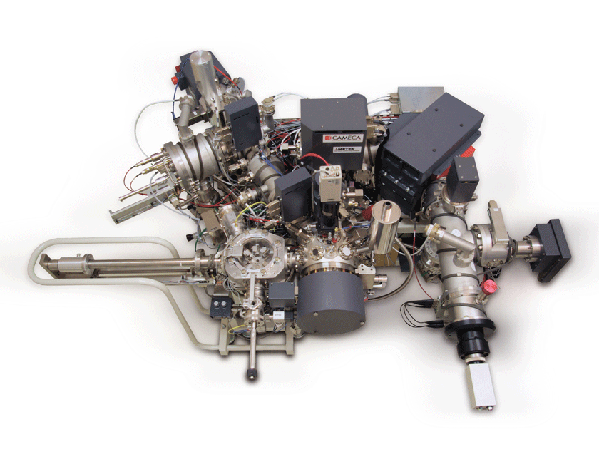
The CAMECA
IMS 7f-Auto is the latest version of our successful IMS xf product line. Learn more about the SIMS technique and CAMECA's instruments by visiting
CAMECA's SIMS Overview.
Authors: Paula PERES (Applications Manager)